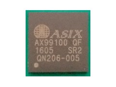
The AX99100 is a single chip solution that fully integrates PCIe 2.0 Gen 1 end-point controller and SerDes with a variety of peripherals such as four High Speed Serial Ports, one Parallel Port, I²C Master, High Speed SPI, Local Bus (ISA-Like) , and GPIOs. It consists of four main configurations such as 4S (PCIe to Quad Serial), 2S+1P (PCIe to Dual Serial and Single Parallel), 2S+SPI (PCIe to Dual Serial and SPI), and LB (PCIe to Local Bus/ISA-Like) for different kinds of applications.
The AX99100, in 68-pin QFN, are available with RoHS compliant package and supports commercial grade operating temperature range from 0 to 70°C and industrial grade from -40 to 85°C. |
规格:
- PCI Express
- Single-lane (X1) PCI Express End-point Controller with PHY integrated
- Compliant with PCI Express 2.0 Gen 1
- Compliant with PCI Express card specifications
- Compliant with PCI Power Management 1.2
- Supports four PCI Express functions
- Supports both legacy and MSI Interrupt
- Supports ASPM Power Management
- Serial Port Interface
- Dual or Quad UARTs
- Supports RS-232/RS-422/RS-485 multiprotocol
- Bi-directional speeds up to 25 Mbps per port
- Full Serial Modem Control
- Supports Hardware, Software Flow Control
- Supports 5, 6, 7, 8 and 9-bit Serial format
- Supports Even, Odd, None, Space and Mark parity
- Supports Custom baud rate by internal PLL or external clock
- Supports On Chip 256 Byte depth FIFOs in Transmit, Receive path of each Serial Port
- Supports remote wakeup and power management features
- Serial Port transceiver shutdown support
- Supports Slow IrDA mode (up to 115200bps) on all Serial Ports
- Supports multi-dro application for 9-bit mode
- Supports DMA burst transfer
- Parallel Port
- Compatible with IEEE 1284 – SPP/Byte/ECP Mode
- SPI Interface
- Programmable SPI clock frequency up to 42MHz
- Supports Mode 0, Mode 1, Mode 2 and Mode 3 timing modes
- Supports MSB/LSB first transfer fashion
- Programmable peripheral chip selec, selecting up to 7 SPI devices
- Supports Non-Burst-Type transfer up to 8 bytes and/or Burst-Type transfer via DMA mode for high performance
- Supports to fragment large data block into several smaller transfers on SPI bus to reduce software loading
- Supports programmable transfer 0 ~ 8 bytes OP-Code field in each transfer automatically to reduce software loading
- Supports wake-up by SWAKEn pin from Slave
- Local Bus Interface
- Supports memory or I/O access through PCIe BAR0/1 to local bus interface, each BAR mapping to local bus\' chip selec (CS0n and CS1n)
- Supports direct access and bus master access (auto-increment and fixed address)
- Supports 8-bit or 16-bit data bus width (little and big endian bus swap)
- Supports up to 2 Kbytes address space and 2 chip selec outputs when separated address/data bus style
- Supports up to 64 Kbytes address space and 2 chip selec outputs when multiplexed address/data bus style
- Supports programmable local chip selec region
- Supports “Slave Request based DMA” access for interfacing with external device with bus master
- Supports clock out, CLKO, up to 62.5MHz
- Supports asynchronous or synchronous Local Bus with required clock output, CLKO
- Supports programmable bus access cycles, self-terminated bus access cycles and back-to-back turnaround cycles
- Supports programmable RSTO, ALE, RDY, DREQ0/1, DACK0/1, CLKO polarity, and INT0/1 level/edge trigger
- Supports wake-up by INT0/1 and DREQ0/1 pins
- Supports I²C Master Interface
- Up to 24 bi-directional GPIO lines including 8 dedicated GPIO and 16 multi-function GPIO
- Integrates on-chip power-on reset circuit
- On Chip 3.3 to 1.2V Regulator
- 68-pin QFN RoHS compliant package
- Operating temperature range: 0 to 70°C or -40 to +85°C
|